- Home
- Tablets
- Tablets News
- Paper thin, flexible tablets and TV displays could be a reality
Paper-thin, flexible tablets and TV displays could be a reality

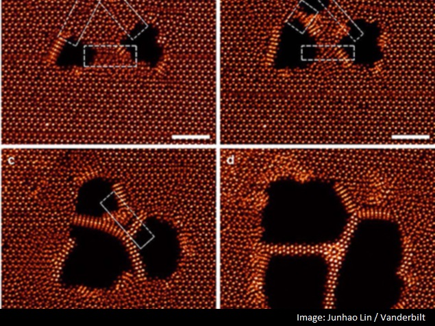
Scientists have used a focused beam of electrons to create some of the smallest nanowires ever made, an advance that paves the way for flexible, paper-thin tablets and television displays.
Junhao Lin, a Vanderbilt University student and visiting scientist at Oak Ridge National Laboratory (ORNL), used a finely focused beam of electrons to create the flexible metallic wires only three atoms wide: one thousandth the width of the microscopic wires used to connect the transistors in today's integrated circuits.
According to Lin's advisor Sokrates Pantelides, University Distinguished Professor of Physics and Engineering at Vanderbilt University, and his collaborators at ORNL, the technique represents an exciting new way to manipulate matter at the nanoscale and should give a boost to efforts to create electronic circuits out of atomic monolayers, the thinnest possible form factor for solid objects.
Lin made the tiny wires from a special family of semiconducting materials that naturally form monolayers.
These materials, called transition-metal dichalcogenides (TMDCs), are made by combining the metals molybdenum or tungsten with either sulfur or selenium.
The best-known member of the family is molybdenum disulfide, a common mineral that is used as a solid lubricant.
Atomic monolayers are the object of considerable scientific interest because they tend to have a number of remarkable qualities, such as exceptional strength and flexibility, transparency and high electron mobility.
Other research groups have already created functioning transistors and flash memory gates out of TMDC materials.
So the discovery of how to make wires provides the means for interconnecting these basic elements.
Next to the transistors, wiring is one of the most important parts of an integrated circuit. Although today's integrated circuits (chips) are the size of a thumbnail, they contain more than 32 kms of copper wiring.
"This will likely stimulate a huge research interest in monolayer circuit design," Lin said.
"Because this technique uses electron irradiation, it can in principle be applicable to any kind of electron-based instrument, such as electron-beam lithography," Lin added.
One of the intriguing properties of monolayer circuitry is its toughness and flexibility.
It is too early to predict what kinds of applications it will produce, but "If you let your imagination go, you can envision tablets and television displays that are as thin as a sheet of paper that you can roll up and stuff in your pocket or purse," Pantelides said.
The study included a group headed by Kazu Suenaga at the National Institute of Advanced Industrial Science and Technology in Tsukuba, Japan. Other collaborators at ORNL, the University of Tennessee in Knoxville, Vanderbilt University, and Fisk University contributed to the project.
The study was published in the journal Nature Nanotechnology.
For the latest tech news and reviews, follow Gadgets 360 on X, Facebook, WhatsApp, Threads and Google News. For the latest videos on gadgets and tech, subscribe to our YouTube channel. If you want to know everything about top influencers, follow our in-house Who'sThat360 on Instagram and YouTube.
Related Stories
- Samsung Galaxy Unpacked 2025
- ChatGPT
- Redmi Note 14 Pro+
- iPhone 16
- Apple Vision Pro
- Oneplus 12
- OnePlus Nord CE 3 Lite 5G
- iPhone 13
- Xiaomi 14 Pro
- Oppo Find N3
- Tecno Spark Go (2023)
- Realme V30
- Best Phones Under 25000
- Samsung Galaxy S24 Series
- Cryptocurrency
- iQoo 12
- Samsung Galaxy S24 Ultra
- Giottus
- Samsung Galaxy Z Flip 5
- Apple 'Scary Fast'
- Housefull 5
- GoPro Hero 12 Black Review
- Invincible Season 2
- JioGlass
- HD Ready TV
- Laptop Under 50000
- Smartwatch Under 10000
- Latest Mobile Phones
- Compare Phones
- Moto G15 Power
- Moto G15
- Realme 14x 5G
- Poco M7 Pro 5G
- Poco C75 5G
- Vivo Y300 (China)
- HMD Arc
- Lava Blaze Duo 5G
- Asus Zenbook S 14
- MacBook Pro 16-inch (M4 Max, 2024)
- Honor Pad V9
- Tecno Megapad 11
- Redmi Watch 5
- Huawei Watch Ultimate Design
- Sony 65 Inches Ultra HD (4K) LED Smart TV (KD-65X74L)
- TCL 55 Inches Ultra HD (4K) LED Smart TV (55C61B)
- Sony PlayStation 5 Pro
- Sony PlayStation 5 Slim Digital Edition
- Blue Star 1.5 Ton 3 Star Inverter Split AC (IC318DNUHC)
- Blue Star 1.5 Ton 3 Star Inverter Split AC (IA318VKU)


