- Home
- Science
- Science News
- Nanowires Could Be LEDs of the Future
Nanowires Could Be LEDs of the Future

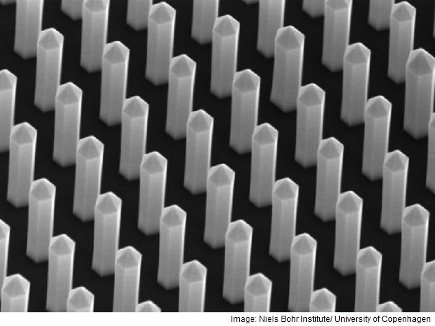
Researchers from the Niels Bohr Institute in Denmark studied nanowires using X-ray microscopy and were able to pinpoint exactly how the nanowire should be designed to give the best properties.
Nanowires are very small - about 2 micrometres high (1 micrometer is a thousandth of a millimetre) and 10-500 nanometres in diameter (1 nanometre is a thousandth of a micrometre).
Nanowires for Light Emitting Diodes (LEDs) are made up of an inner core of gallium nitride (GaN) and a layer of indium-gallium-nitride (InGaN) on the outside, both of which are semiconducting materials.
"The light in such a diode is dependent on the mechanical strain that exists between the two materials and the strain is very dependent on how the two layers are in contact with each other," said Robert Feidenhans'l, professor and head of the Niels Bohr Institute at the University of Copenhagen.
"We have examined a number of nanowires using X-ray microscopy and even though the nanowires should in principle be identical, we can see that they are different and have very different structure," Feidenhans'l said.
The studies were performed using nanoscale X-ray microscopy in the electron synchrotron at DESY in Hamburg, Germany.
The method is usually very time consuming and the results are often limited to very few or even a single study subject.
But researchers have managed to measure a series of upright nanowires all at once using a special design of a nanofocused X-ray without destroying the nanowires in the process.
"We measured 20 nanowires and when we saw the images, we were very surprised because you could clearly see the details of each nanowire. You can see the structure of both the inner core and the outer layer," said Tomas Stankevic, a PhD student at the Niels Bohr Institute.
"If there are defects in the structure or if they are slightly bent, they do not function as well. So we can identify exactly which nanowires are the best and have the most efficient core/shell structure," Stankevic said.
The nanowires are produced by a company in Sweden and this new information can be used to tweak the layer structure in the nanowires.
Feidenhans'l said that there is great potential in such nanowires. They will provide a more natural light in LEDs and they will use much less power. In addition, they could be used in smartphones, televisions and many forms of lighting.
The researchers expect that things could go very quickly and that they may already be in use within five years.
The research was published in the journal ACS Nano.
For the latest tech news and reviews, follow Gadgets 360 on X, Facebook, WhatsApp, Threads and Google News. For the latest videos on gadgets and tech, subscribe to our YouTube channel. If you want to know everything about top influencers, follow our in-house Who'sThat360 on Instagram and YouTube.
Related Stories
- Samsung Galaxy Unpacked 2025
- ChatGPT
- Redmi Note 14 Pro+
- iPhone 16
- Apple Vision Pro
- Oneplus 12
- OnePlus Nord CE 3 Lite 5G
- iPhone 13
- Xiaomi 14 Pro
- Oppo Find N3
- Tecno Spark Go (2023)
- Realme V30
- Best Phones Under 25000
- Samsung Galaxy S24 Series
- Cryptocurrency
- iQoo 12
- Samsung Galaxy S24 Ultra
- Giottus
- Samsung Galaxy Z Flip 5
- Apple 'Scary Fast'
- Housefull 5
- GoPro Hero 12 Black Review
- Invincible Season 2
- JioGlass
- HD Ready TV
- Laptop Under 50000
- Smartwatch Under 10000
- Latest Mobile Phones
- Compare Phones
- Moto G15 Power
- Moto G15
- Realme 14x 5G
- Poco M7 Pro 5G
- Poco C75 5G
- Vivo Y300 (China)
- HMD Arc
- Lava Blaze Duo 5G
- Asus Zenbook S 14
- MacBook Pro 16-inch (M4 Max, 2024)
- Honor Pad V9
- Tecno Megapad 11
- Redmi Watch 5
- Huawei Watch Ultimate Design
- Sony 65 Inches Ultra HD (4K) LED Smart TV (KD-65X74L)
- TCL 55 Inches Ultra HD (4K) LED Smart TV (55C61B)
- Sony PlayStation 5 Pro
- Sony PlayStation 5 Slim Digital Edition
- Blue Star 1.5 Ton 3 Star Inverter Split AC (IC318DNUHC)
- Blue Star 1.5 Ton 3 Star Inverter Split AC (IA318VKU)


