- Home
- Laptops
- Laptops News
- Intel Says 'Tick Tock' Strategy Isn't Working Anymore
Intel Says 'Tick-Tock' Strategy Isn't Working Anymore
By Jamshed Avari | Updated: 23 March 2016 13:37 IST

Click Here to Add Gadgets360 As A Trusted Source

Advertisement
Intel will stop following its two-year "tick-tock" development model, according to details contained within a routine report published by the company. The chipmaker's most recent form 10-K, a financial document filed annually with the United States Securities and Exchange Commission, outlines all of its business operations and any details potentially relevant to investors and regulators.
The most interesting section deals with Intel's R&D efforts. The company says it spent $12.1 billion on designing and manufacturing electronic circuits in 2015, compared to $11.5 billion in 2014. Specific areas of improvement named in the report are energy efficiency, system-level integration, security, scalability for multi-core architectures, system manageability, and ease of use.
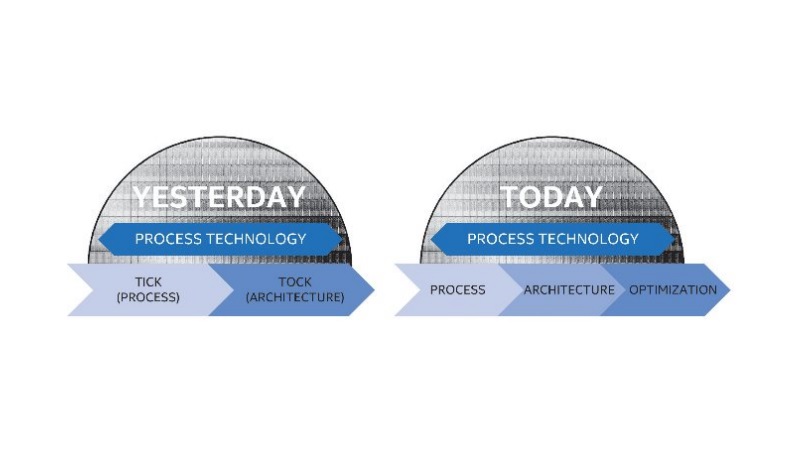
The document, first spotted by The Motley Fool, then outlines a new cadence for product development, as opposed to the two year alternating "tick-tock" model which has served for the past decade. Rather than changing its manufacturing process one year and then architecture the next, there is now a third step: optimisation. The document states "We expect to lengthen the amount of time we will utilise our 14nm and our next-generation 10nm process technologies, further optimising our products and process technologies while meeting the yearly market cadnce for product introductions".
This lines up with last year's public announcement that development of the 10nm process would take longer than anticipated, and that the current 14nm process, which debuted with the Broadwell architecture and was adopted for Skylake, will carry forward to another product generation, code named Kaby Lake, in late 2016.
Kaby Lake was seen at the time as a stopgap measure to allow Intel to release a new lineup on schedule without having the 10nm process ready. Now, the document indicates that Kaby Lake will have "key performance enhancements" as compared to Skylake, which means it won't be just a minor refresh to tide the company over.
Intel cites Moore's Law as one reason to lay "tick-tock" to rest. Other R&D goals include significantly reducing transistor leakage, lowering active power requirements, and increasing transistor density to allow for ever-smaller packages. Intel is also funding research of extreme ultraviolet and deep-immersion lithography.
According to Intel's SEC filing, the company had 107,300 employees as of the end of 2015, of whom 51 percent are located in the US. Its facilities around the world add up to 56 million square feet of space. Hewlett-Packard Company, which recently split into two entities, is named as Intel's biggest customer in 2015, accounting for 18 percent of its net revenue, followed by Dell at 15 percent.
Comments
Get your daily dose of tech news, reviews, and insights, in under 80 characters on Gadgets 360 Turbo. Connect with fellow tech lovers on our Forum. Follow us on X, Facebook, WhatsApp, Threads and Google News for instant updates. Catch all the action on our YouTube channel.
Further reading:
10nm, 14nm, Broadwell, CPU, Intel, Intel research, Intel roadmap, Intel strategy, Kaby Lake, Skylake, processors, tick tock
Related Stories
Popular on Gadgets
- Samsung Galaxy Unpacked 2026
- iPhone 17 Pro Max
- ChatGPT
- iOS 26
- Laptop Under 50000
- Smartwatch Under 10000
- Apple Vision Pro
- Oneplus 12
- OnePlus Nord CE 3 Lite 5G
- iPhone 13
- Xiaomi 14 Pro
- Oppo Find N3
- Tecno Spark Go (2023)
- Realme V30
- Best Phones Under 25000
- Samsung Galaxy S24 Series
- Cryptocurrency
- iQoo 12
- Samsung Galaxy S24 Ultra
- Giottus
- Samsung Galaxy Z Flip 5
- Apple 'Scary Fast'
- Housefull 5
- GoPro Hero 12 Black Review
- Invincible Season 2
- JioGlass
- HD Ready TV
- Latest Mobile Phones
- Compare Phones
Latest Gadgets
- Itel Zeno 200
- OnePlus Nord CE 6 Lite
- OnePlus Nord CE 6
- Honor Play 70C
- Honor Play 80 Plus
- Moto G47
- Motorola Razr 2026
- Motorola Razr+ 2026
- HP OmniBook 5 (2026)
- HP OmniBook Ultra 14 (Snapdragon, 2026)
- HP OmniPad 12
- Acer Iconia iM11-22M5G
- NoiseFit Halo 3
- NoiseFit Diva Araya
- Lumio Vision 9 (2026)
- Lumio Vision 7 (2026)
- Asus ROG Ally
- Nintendo Switch Lite
- Blue Star 1.5 Ton 5 Star Inverter Split AC (IA518ZXUS)
- Blue Star 1.5 Ton 3 Star Inverter Split AC (IA318ZXU)
© Copyright Red Pixels Ventures Limited 2026. All rights reserved.


