- Home
- Cameras
- Cameras News
- New Camera Sensor Could Turn a Smartphone Into a 3D Scanner
New Camera Sensor Could Turn a Smartphone Into a 3D Scanner

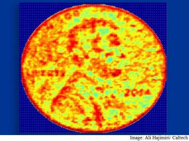
This feat may soon be possible because of a new tiny high-resolution 3D imager developed by researchers at California Institute of Technology.
The cheap, compact yet highly accurate new device known as a nanophotonic coherent imager (NCI) uses inexpensive silicon chip less than a millimetre square in size.
The NCI provides the highest depth-measurement accuracy of any such nanophotonic 3D imaging device.
"The small size and high quality of this new chip-based imager will result in significant cost reductions, which will enable thousands of new uses for such systems by incorporating them into personal devices such as smartphones," explained Ali Hajimiri, Thomas G. Myers professor of electrical engineering.
The new chip uses an established detection and ranging technology called LIDAR, in which a target object is illuminated with scanning laser beams.
The first proof of concept of the NCI has only 16 coherent pixels, meaning that the 3D images it produces can only be 16 pixels at any given instance.
In the future, Hajimiri said, that the current array of 16 pixels could also be easily scaled up to hundreds of thousands.
The imager could be applied to a broad range of applications from very precise 3D scanning and printing to helping driverless cars avoid collisions to improving motion sensitivity in superfine human machine interfaces, said the paper that appeared in the journal Optics Express.
Get your daily dose of tech news, reviews, and insights, in under 80 characters on Gadgets 360 Turbo. Connect with fellow tech lovers on our Forum. Follow us on X, Facebook, WhatsApp, Threads and Google News for instant updates. Catch all the action on our YouTube channel.
Related Stories
- Samsung Galaxy Unpacked 2026
- iPhone 17 Pro Max
- ChatGPT
- iOS 26
- Laptop Under 50000
- Smartwatch Under 10000
- Apple Vision Pro
- Oneplus 12
- OnePlus Nord CE 3 Lite 5G
- iPhone 13
- Xiaomi 14 Pro
- Oppo Find N3
- Tecno Spark Go (2023)
- Realme V30
- Best Phones Under 25000
- Samsung Galaxy S24 Series
- Cryptocurrency
- iQoo 12
- Samsung Galaxy S24 Ultra
- Giottus
- Samsung Galaxy Z Flip 5
- Apple 'Scary Fast'
- Housefull 5
- GoPro Hero 12 Black Review
- Invincible Season 2
- JioGlass
- HD Ready TV
- Latest Mobile Phones
- Compare Phones
- Honor Play 80
- Nord 6
- Honor X80i
- Honor Play 80 Pro
- Redmi Note 15 SE 5G
- Redmi A7 Pro
- OPPO K15 Pro
- OPPO K15 Pro+
- Xiaomi Book Pro 14
- MacBook Neo
- Vivo Pad 6 Pro
- Lenovo Legion Y700 Gen 5
- boAt Valour Watch 1R
- Xiaomi Watch S5
- Xiaomi QLED TV X Pro 75
- Haier H5E Series
- Asus ROG Ally
- Nintendo Switch Lite
- Haier 1.6 Ton 5 Star Inverter Split AC (HSU19G-MZAID5BN-INV)
- Haier 1.6 Ton 5 Star Inverter Split AC (HSU19G-MZAIM5BN-INV)


